- +91-11-9810681132, 9868532156
- info@mittalenterprises.com
Note: No part of this website may be reproduced, stored in a retrieval, or transmitted in any form or by any mean
Note: No part of this website may be reproduced, stored in a retrieval, or transmitted in any form or by any mean

Objective: MEASUREMENT of Energy Band Gap of Semiconductors like Si, Ge etc using p-n junction diodes and LEDs

|
|||
|
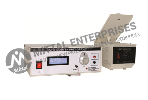
Forbidden Energy Gap Kit Forbidden Energy Gap Kit, the Forward biased voltage of a silicon/germanium diode or LED is studied as a function of temperature. The results can be used to evaluate Forbidden Energy Gap of Silicon, Germanium and L.E.D. The kit is self contained and needs no additional equipment. Current and Voltage are measured using digital Micro- ammeter and digital Voltmeter respectively. The diode under investigation is to be connected to the main unit. With the help of Hot air oven and oil, temperature of sample is raised and corresponding voltages are measured. From Slope (a) and intercept (b) of graph between voltage and temperature, Energy Gap is calculated using eqn (2). INSTRUMENT The apparatus consists of main unit having digital voltmeter (0-9.99V dc) and micro ammeter (0-999 µA dc), Digital Temperature Indicator, highly stabilized variable power supply, Samples (Ge, Si, LED), Energy controlled hot air oven, Silicon Oil and Thermocouple. |
|||
| Enquiry | |||